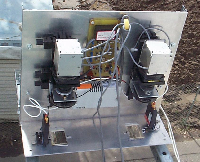
Figure 1: Top View of the System
| Current Prototype | Fourth Prototype | Third Prototype | Second Prototype | First Prototype |
Based on the first prototype, the second prototype displays a lot of changes. As can be seen from Figure 1, below, the most noticable change is the overall design of the Laser Based Detection System (LBDS). The whole system is now contained within a box incluser were as before, the lenses of the system protruded from the bottom of the system. New mechanical fixtures have been used to fasten the lenses and APD array down. Figure 2, below, gives a system overview of the second prototype.
Figure 1: Top View of the System
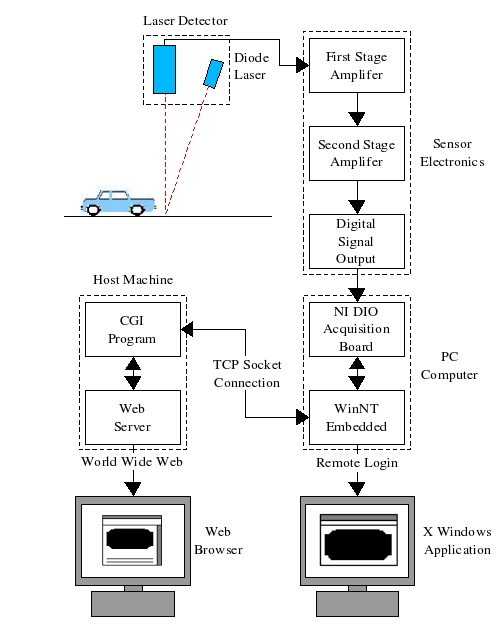
Figure 2: System Overview
The first protorype showed that the theory behind the LBDS is sound. It was able to find the amount of time a vehicle was under the seonsor consistently. It, however, did not function as well as planned in all areas. During testing, some problems were found. While minor problems where fixed, the majority of the problems were addressed in the second prototype.
The second-generation prototype uses many commercially available available parts instead of having to design and manufacture all of the parts in-house.
Laser and Sensor Optics
The optics have not changed compared to the first prototype. The same lenses and APD array are used. Only 4-elements of the APD array are currently being used.
System Electronics
The second prototype outputs a digital signal instead of an analog signal as was done with the first prototype. Changing the system to digtal greatly reduces the crititcal height of the system and allows multiple channels to be read in one cycle which saves valuable computing time. A TTL logic circuit, which is triggered by laser pulses to generate digital output, is used to replace a sample-and-hold amplifier for signal peak detection. This method improves the time response of the system. Figure 3, below, shows a diagram of the electronic hardware. Changing the signal from an analog to a digital signal allows for much less noise from the circuitry. A electrical circuit diagran is shown in Figure 4, below. A two stage amplifer is used to amplify the nano-amp signal from the APD array to a 2.5 Volt signal. A microchip is used to change the 2.5 Volt signal to a 5 Volt high and 0 Volt low digital signal.
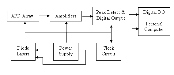
Figure 3: Diagram of the Electronic Hardware
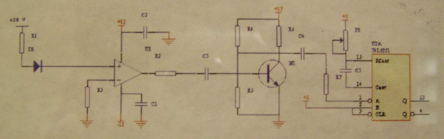
Figure 4: Electronic Circuit
Data Acquisiton System
Since the outputs of the sensor circuits are digital signals, the A/D converter is no longer needed. A general-purpose low-cost digital I/O board PCI-DIO-96 from National Instruments is used as an input interface between the sensor circuitry and the computer system. This digital I/O has 96 channels of configurable input/output, so it is suitable for our system when all 48 channels of signal are required.
This board has 96-channel programmable digital. We chose Embeded WinNT instead of the Lynx OS due to driver availability. In order to utilize the PCI-DIO-96 board, we would have to create our own Lynx OS device drivers.